
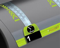
- Automotive
- Battery Lamination
- Ball Grid Array (BGA)
- Bed / Mattress
- Biomechanics
- Brake Pad
- Body Mapping
- Bolted Joint
- Bolt Switch
- Bolt Pressure Indicator
- Calender Press
- Clamping
- Composite Layup
- Connector
- Clutch
- Door Seal
- Ergonomics
- Flex
- Foot
- Foot Insole
- Fuel Cell Manufacturing
- Gasket Sealing
- Glove
- Hand Grip Pressure
- Heat Sealing
- Heat Sink
- Human Body Interface
- Impact Study
- Injection Molding
- LCD Bonding
- Metal Stamping
- Lamination Press
- Nip Impression
- Patient Movement Monitor
- Podiatry / Orthotics
- Printed Circuit Board
- Saddle Fitting
- Seating
- Soil-Structure Interaction
- Solar Cells
- Spray
- Squeezable Tube
- Tire Tread Footprint
- Temperature Mapping
- Ultrasonic Welding
- UV Light Measurement
- Vest / Body Armor
- Wafer Bonding
- Wafer Polishing
- Windshield Wiper
- Squeegee
- Other Applications
- Fujifilm Prescale
- Fujifilm Thermoscale
- Tactilus
- Nip Roller Products
- Topaq
- Mold-Align
- Pressurex-micro
- TemprX
- Thermex
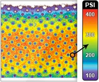
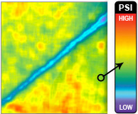
Fujifilm Prescale®
Fujifilm Prescale is a unique, affordable and easy to use tool that reveals the distribution and magnitude of pressure between any two contacting, mating or impacting surfaces. This Tactile Pressure Indicating Sensor Film is extremely thin (4 to 8 mils) which enables it to conform to curved surfaces. Fuji Prescale Film is ideal for invasive intolerant environments and tight spaces not accessible to conventional electronic transducers.
Click here to read more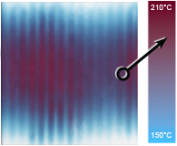
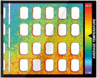
Fujifilm Thermoscale®
Thermoscale® is a unique tool that indicates temperature level and distribution between any two contacting surfaces. The most unique quality of Thermoscale® is that is goes where no other IR camera or temperature gauge can ever go - on the surface of the heated object and in between two contacting surfaces!
Click here to read more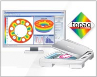
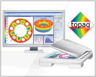
Topaq® Pressure Analysis System
Used in conjunction with Fujifilm Prescale pressure indicating films, Topaq provides a quick, yet thorough analysis of the pressure distribution and magnitude between any two surfaces that come into contact... read more
Topaq® Service
Need to obtain statistical data and enhanced digital visuals of your Fujifilm Prescale? Let our technicians analyze your pressure exposed impressions with the all new Topaq Pressure Analysis System... read more
Mold Align®
Mold-Align is a unique, affordable and easy to use tool that reveals pressure distribution between mold platens. Mold-Align paper, which changes color relative to the amount of contact force. It is an extremely economical and practical solution for determining proper mold alignment... read more
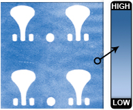
Pressurex-micro®
Pressurex-mirco is a unique, affordable and easy to use tool that reveals relative pressure distribution between two contacting, mating or impacting surfaces. This pressure indicating sensor film is thin (20 mils) which enables it to conform to curved surfaces. It is ideal for invasive intolerant environments and tight spaces not accessible to conventional electronic transducers... read more
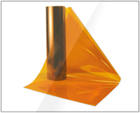
TemprX®
Fuji Prescale film is a unique, affordable and easy to use tool that reveals the distribution and magnitude of pressure between any two contacting, mating or impacting surfaces. With the use of TemprX thermal protection polyimide film it can be used in applications that reach high temperatures... read more
Thermex®
Thermex® is a unique temperature indicating material. As thin as a standard sheet of paper, Thermex changes color to reveal relative temperature distribution between any two contacting surfaces. Upon exposure to temperature, the Thermex® sheet instantaneously and permanently changes color, with the intensity of that color directly related to the temperature it was exposed to. This allows Thermex to reveal spot high or low temperature zones. Thermex® is inexpensive, precise and disposable... read more
- Topaq Service
- Encasement
- In-House Consulting
- Laser Cutting
- Leasing
- R&D Engineering
Topaq® Service
Need to obtain statistical data and enhanced digital visuals of your Fuji Prescale films? Let our technicians analyze your pressure exposed impressions with the all new Topaq Pressure Analysis System.
Click here to read more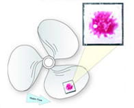
Encasement Service
Our new Encasement Service for Pressure Indicating Film offers engineers in the flexo, converting and packaging industries the ability to have Fujifilm Prescale protected so that it can measure contact pressure.
Click here to read more
In-House Consulting
Sensor Products now introduces our new in-house surface stress analysis service. All you need to do is send your part, machine, fixture or assembly to us and weŌĆÖll do the rest. Via video-conferencing you can view the results of our analysis practically in real-time.
Click here to read more
Laser Cutting
We offer custom laser cutting services for tactile pressure sensor film to measure contact pressure.
Click here to read more
Leasing Options
Sensor Products offers a variety of products that are available for short and long term lease. A lease will enable you to gain access to the benefits of our products without the commitment to buy. Furthermore, after your analysis you can also send the session data back to us for a more in-depth review and critique.
Click here to read more
R&D Engineering
Sensor Products has a highly dedicated team of talented engineers with 25 years of combined experience in the niche discipline of tactile surface sensing. Your project will be supervised by a product manager who will be your direct contact, and worked upon by our staff consists of material, mechanical, and PHD level electrical engineers.
Click here to read more


